
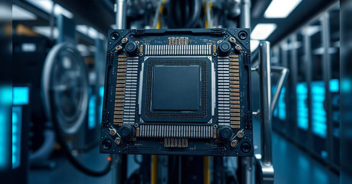
The advanced chip packaging industry is undergoing a historic transformation, driven by unprecedented demand for artificial intelligence (AI) and high-performance computing (HPC). This shift is fundamentally reshaping global semiconductor investment priorities and supply chain dynamics.Global venture capital investment in AI exceeded $100 billion in 2024, marking an 80 per cent increase from $55.6 billion in 2023, with 33 per cent of all global venture funding directed into AI companies. US chip startups alone raised nearly $3 billion in AI-related funding in 2024, a 123 per cent jump from approximately $1.3 billion in 2023.
Capacity and Investment Trends
Asia-Pacific’s advanced packaging capacity has quadrupled in less than two years due to AI demand, solidifying the region’s dominance in CoWoS, HBM, and heterogeneous integration, which are critical for AI data centre GPUs. The US CHIPS and Science Act has catalysed over $450 billion in private sector investment since 2022, with beneficiaries including TSMC ($6.6 billion in funding for over $65 billion Arizona investment), Amkor Technology ($400 million for a $2 billion advanced packaging campus), and SK hynix ($458 million for a $3.87 billion HBM packaging facility in Indiana).Generative AI funding nearly doubled from $24 billion in 2023 to approximately $45 billion in 2024, further accelerating demand for CoWoS-integrated GPU packages and high-bandwidth memory (HBM) stacks. NVIDIA GPU production for data centres is projected to reach 7.4 million units by the end of 2026, placing immense pressure on packaging supply chains. TSMC’s CoWoS capacity is substantially booked through 2026.
Emerging Technologies and Geopolitical Implications
CoWoS has become an industry standard for AI accelerator packaging. Emerging technologies such as 2.5D and 3D heterogeneous integration, LPDDR6-PIM, photonic interconnects, hybrid bonding, and panel-level packaging are redefining performance for on-device and data centre AI. Apple is targeting a transition to discrete DRAM packaging by 2026 to meet mobile AI bandwidth requirements.The structural forces in advanced chip packaging extend beyond immediate AI infrastructure build-out, with acute and systemic supply constraints. European semiconductor packaging infrastructure remains critically underdeveloped, creating strategic dependence on Asia-Pacific. China’s $47 billion “Big Fund III” and South Korea’s K-Semiconductor Strategy, targeting $450 billion by 2030 for HBM and AI accelerator packaging, highlight the geopolitical urgency for domestic self-sufficiency. Japan’s Rapidus has secured approximately $5.2 billion in government funding for 2-nanometer and 1-nanometer process technologies, while Silicon Box is investing up to $3.6 billion, supported by $1.4 billion in EU aid, for a panel-level packaging foundry in Northern Italy. These developments underscore advanced packaging’s repositioning as a mission-critical strategic asset in national industrial policy and corporate technology roadmaps.










Leave a Reply